3D Substrate
A substrate that is a fusion of many processing and materials technologies for module miniaturization and multi functionality
A wide variety of optional technologies is available
Product Outline
- Excellent copper plating technology; can be made to match any shape
- Miniaturization and compactness are possible while maintaining stable high frequency characteristics, so finds a lot of uses in sensors
Manufacturing locations:Ishioka Plant
Features
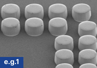
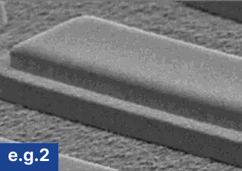
01Variety of shapes possible
With excellent copper plating technology, flexible bump formation is possible.
Example 1) Height: 180μm / Diameter: 250μm
(Minimum: height: 150μm / Diameter 170μm)
Example 2) Height: 20μm / Size: 0.15 x 9.0mm
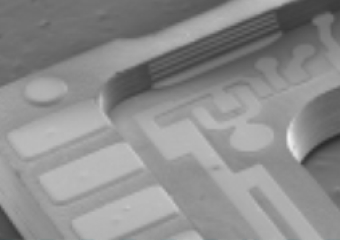
02Product becomes more compact and high frequency characteristics improved
Cavity structure is made possible by high precision counterboring. Components can be mounted inside the cavity directly, allowing for more compact design and improved high frequency performance.
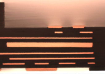
03Smaller size and space saving by using wire bondable stack vias
Our high-precision 3D circuit boards are compact, featuring stacked vias that allow for stacking while ensuring flatness. And wire bonding is possible, so the product can be made more compact while ensuring reliability.
Typical applications
Module substrates

Lincstech’s high density, high reliability substrates are ideal for the high performance power modules, multi chip modules, and other modules essential for smartphones and other electronic devices.
Sensors

High accuracy sensors are indispensable in applications like self-driving vehicles, industrial equipment and robots. Lincstech’s substrates with high density signal lines contribute to the development of smaller, more accurate sensors.
LEDs

Energy-efficient LEDs have become the mainstay in the lighting of modern society. Lincstech’s substrates, with their small form factor and complex wiring, play a part in developing brighter, smaller LED products.
