- TOP
- Products
Products
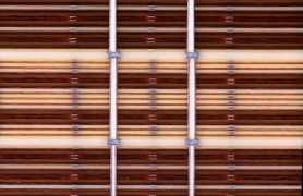
Our goal is to place no restrictions on the form of development. We manufacture the MWB (multi wiring board)
using our original technology and other printed wiring boards (PWBs) for use in a broad range of applications.
Product Lineup
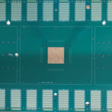
MWB
(Multi Wiring Board)
Stable high frequency characteristics; Suitable for products requiring high wire count and high degree of integration.
Shimodate Plant
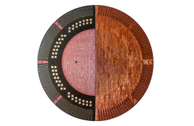
Multi Layer Board
(High density high layer count MLB)
High layer count and density made possible by stacking, drilling, and plating technologies and high precision electrical and scale simulation.
Shimodate PlantLCS
Thin build up substrate
PWB made by our original processing technology for a thin board with high layer count.
Ishioka Plant
3D Substrate
PWB that is a fusion of a variety of PWB processing and material technologies.
Ishioka Plant
-
High density interconnect (HDI) wiring boards
Shimodate PlantLCS
-
Multilayer
wiring boards
(20 layers and fewer)Shimodate PlantIshioka PlantLCSYGA
-
Double sided
wiring boardsShimodate PlantIshioka PlantYGA
-
Aluminum
wiring boardsYGA
-
Single sided
wiring boardsYGA
Pricing
Price depends on the product and required characteristics.
Please feel free to contact us to discuss your needs.
Search by characteristics
 Thin
Thin
When developing products that pack a lot of features in a compact form factor, “smaller” and “thinner” become even more critical. Our original processing technology makes thin wiring boards possible.
Our technology has applications in module substrates, sensors, LEDs, IC testers, probe cards, performance boards, switchboards, servers, industrial equipment, medical devices, and many more.
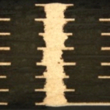
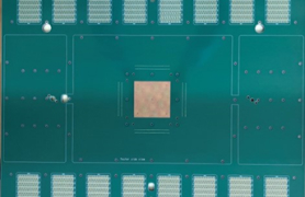
 High layer count / High density
The next generation of computers and sensors will require printed wiring boards with higher layer count and density. Lincstech’s MWB and board-to-board connected wiring boards offer several times the density of conventional multilayer wiring boards to support engineers in the development of these demanding products.
Applications include semiconductor inspection equipment, probe cards, switchboards, high-end computers, sensors, and modules.
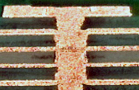
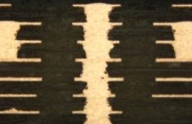
 High speed transmission, high frequency
With developments like 5G and 6G, data transmission speeds in computers and smartphones have increased rapidly. Improving data rates in these devices requires high frequency PWBs that can transmit data at higher and higher speeds. Lincstech’s PWBs have excellent characteristics particularly at high frequencies, and are used by the biggest makers in the communications business.
These PWBs are used in modules for smartphones, switchboards, high end computers, servers, industrial equipment, and communications equipment.
 Heat dissipation
Device miniaturization and expansion of frequency ranges makes the circuit’s heat dissipation an issue. Printed wiring boards, with their excellent heat dissipation characteristics, are a vital component in device miniaturization and increased functionality. Lincstech offers printed wiring boards that have both high density and excellent heat dissipation.
Applications include modules, sensors and LEDs used in smartphones and other devices.
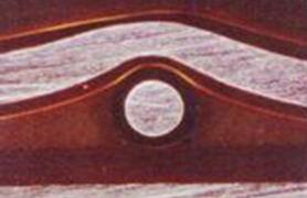
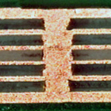
 3D circuit structures
As devices become smaller, the need to embed complex components in a small space has arisen. Lincstech has employed cavity construction, wire bondable stacked vias, bump forming and other technologies to realize 3D printed wiring boards with higher design freedom.
They are used in all kinds of modules, sensors and LEDs.
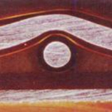
 Embedded capacitors
Power consumption of high speed electronic circuits is increasing, and embedded capacitors play an important role in power line stability. Lincstech’s PWBs can also allow for embedded capacitors and other specialized specifications.
This technology finds applications in modules for servers, routers, storage and other IT devices.
Product
-
-
High density interconnect (HDI) wiring boards
-
We make PWBs tailored to your needs.
From customization of existing products to collaborative development,
we are flexible in addressing customer needs. Please talk with us about your needs.
We are confident not only in our product features and quality, but also in the speed of our response.
Here, we introduce our manufacturing flow in detail.
Search by application
Probe cards
The probe cards used in semiconductor manufacturing quality inspections by their nature demand high reliability PWBs.
IC testers
Lincstech boasts a high share in semiconductor inspection fixtures, so you can leave the manufacture of your printed wiring boards to us with confidence.
IT cloud servers
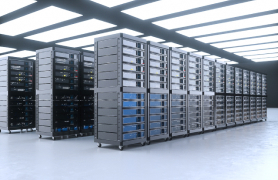
The proliferation of cloud storage and increasing speed of internet lines makes the processing speed of servers and other communications equipment all the more important.
Lincstech’s PWBs for servers realize high speed transmission by reduced signal line resistance and stable electrical characteristics.
Industrial equipment
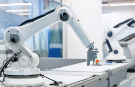
Automation and productivity improvements demand printed wiring boards that are both dense and highly reliable.
With our long track record of business with customers of all kinds, Lincstech supports your development work with high quality PWB manufacture.
Automotive

Electronic control units (ECU), battery management and monitoring units, automotive chargers, fuse boxes, battery modules and other systems demand high reliability printed wiring boards to ensure the vehicle’s safe operation.
Lincstech considers a vehicle’s broad requirements not only for high density and impedance control, but also high current and heat conduction and dissipation.
Sensors and LEDs
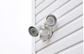
Sensors and LEDs require both high precision and miniaturization.
Lincstech offers a broad lineup of printed wiring boards that are compact and have high density signal lines.
Home appliances
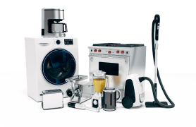
When developing user-friendly and convenient IoT home appliances, printed wiring boards that fit the needs of each kind of appliance are required.
Lincstech leverages our relationships with major home appliance electronic components manufacturers to provide wiring boards of high reliability and stability.
Product
-
-
Multilayer wiring boards
(20 layers and fewer) -
Double sided wiring boards
-
Single sided wiring boards
-
Communications

High performance modules are indispensable in communications devices like smartphones.
Lincstech’s printed wiring boards have high density and high reliability, making them well-suited to communications devices and modules.
Medical devices
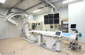
The most important requirement of devices used in the medical field is that they continue to function reliably in any environment.
Lincstech’s printed wiring boards have excellent connection reliability and thermal dissipation characteristics and find applications in medical devices like pace makers and defibrillators.
Amusement

In the amusement industry, the quantity of boards used varies seasonally, and there’s a tendency toward tight deliveries and large, sudden orders.
Lincstech has built a system that can respond adeptly to such rapid changes in demand, and offer attractive price and delivery even for urgent orders.
Product
-
-
Multilayer wiring boards
(20 layers and fewer) -
Double sided wiring boards
-
We manufacture PWBs to your specifications
Whether it’s customization or recreation of existing designs or collaborative development,
we respond to customer needs flexibly. Please do not hesitate to consult with us.
We at Lincstech are confident not only in our technology and quality, but also in our speed of response.
Here, we introduce our manufacturing flow.
