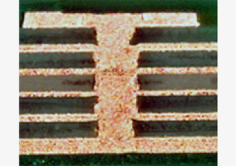
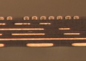
Thin build up substrate
Leading edge substrates made by a combination of ultra-thin build up module substrates and ultra-fine circuit technology
Product Outline
- Substrates that use our original processing technology to achieve high density and thinness; for use in multilayer substrates
- Odd layer count build up substrate (full stack up structure) for excellent heat dissipation
- Environmentally-friendly, using halogen-free materials
Manufacturing locations:Ishioka Plant
Features
01Multilayer substrates can be made thin.
Uses 15μm pre-preg, making wiring boards as thin as 140μm possible
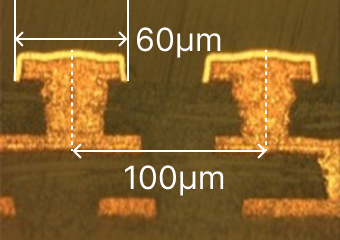
02These substrates have high density, despite being so thin, by realizing narrow pitch.
The Interstitial Via Holes (IVH) in the build up layers are fine pitch. High density, with pitches down to 100μm, are possible to support signals up to 60GHz.
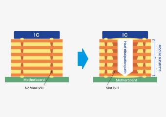
03Heat dissipation is excellent.
Stacked vias realized with copper plating technology. And with slot stacked vias, we can offer substrates with excellent heat dissipation.
04Material is environmentally-friendly.
Constructed of halogen-free material.
Technology roadmap
Unit [ μm ]
※The table can be viewed by scrolling left and right.
| Design item | 2023 | 2024 | 2025 | |
|---|---|---|---|---|
| Line/Space |
20/40 |
20/20 |
||
| Laser via | Via dia.(Min) |
30 |
20 |
|
| Land dia.(Min) |
90 |
80 |
70 |
|
| Land dia.*1(Min) |
80 |
70 |
60 |
|
| Via pitch |
130 |
120 |
100 |
|
| 6L stack up*2 (Au-Au) |
160(Type) |
140(Type) |
130(Type) |
|
| Stack up design |
|
|
|
|


*1) Only for outer layer
*2) PP thickness might be limited upon pattern design and remaining copper ratio
Typical applications
Module substrates

Lincstech’s high density, high reliability substrates are ideal for the high performance power modules, multi chip modules, and other modules essential for smartphones and other electronic devices.
Sensors

High accuracy sensors are indispensable in applications like self-driving vehicles, industrial equipment and robots. Lincstech’s substrates with high density signal lines contribute to the development of smaller, more accurate sensors.
LEDs

Energy-efficient LEDs have become the mainstay in the lighting of modern society. Lincstech’s substrates, with their small form factor and complex wiring, play a part in developing brighter, smaller LED products.
