MLB
(High density high layer count MLB)
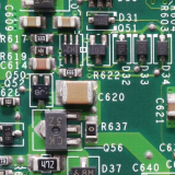
Printed wiring boards realizing high layer count and high density
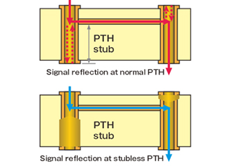
Excellent high frequency characteristics achieved by a combination of back drilling and high frequency materials
Product Outline
- Up to 96 layers and 7.4mm thickness (actual max.)
Many parts can be mounted while maintaining high yield and circuit formation accuracy. - PWBs with excellent throwing power and high quality
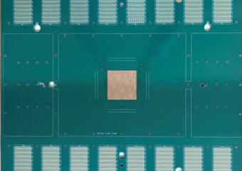
- Product size up to 633 x 550mm. Perfectly suited for use in semiconductor inspection fixtures and communications systems.
- Suitable for high speed communications and high frequency characteristics, strong introduction record in server and cloud systems
Manufacturing locations:
Shimodate PlantLCS
Features
01Up to 96 layers and 7.4mm thickness
High layer count and high density
Uses many of our original technologies in lamination, drilling, plating and others in the manufacturing process. We also perform highly accurate simulations. With these technologies, we realize high layer count and high density characteristics.
02Excellent high speed communications and high frequency performance
By a combination of stubless structure by back drilling and high frequency materials, high frequency electrical characteristics are excellent, making it suitable for high speed communications.
03Excellent throwing power (uniform plating)
Excellent throwing power is achieved with our original electroless copper plating technology. These PWBs deliver high performance.
04Product size up to 633 x 550mm
Recommended for large boards
Sizes up to 633 x 550mm are possible, making it suitable for use in semiconductor inspection fixtures and communications devices
Dimensions Evaluation Board Measured Values vs. Specifications
(633.0×523.4mm)
※The table can be viewed by scrolling left and right.
| Item | Condition ・ Method |
Unit | Spec./ Target |
Result | |
|---|---|---|---|---|---|
| E-679 (FR-4) | MEGTRON 6 | ||||
| Thickness | Micrometer | mm | 7.4±0.6 | Avg.7.285 | Avg.7.317 |
| Warpage | Thickness gauge | mm | ≦1 | Max.0.5 | Max.0.5 |
| BGA Flatness |
3D CMM | mm | ≦0.05 | Max.0.007 | Max.0.057 |
| Solder mask opening dia. |
3D CMM | mm | 0.40±0.05 | Avg.0.394 | Avg.0.402 |
| Plating Thickness (TH) |
Cross-section | μm | Avg. over 20 | Avg.26.7 | Avg.27.5 |
| Characteristic impedance (Z0) |
TDR | Ω | 50±5 | 47.6~49.0 | 47.8~49.5 |
Typical applications
Probe cards
Probe cards are fixtures used to check the quality of wafers used in the semiconductor manufacturing process. The importance of inspection precision is increasing along with semiconductor demand. Lincstech’s printed wiring boards have the top share in semiconductor inspection processes.
IC testers
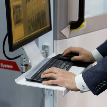
These fixtures are used in the quality and condition tests in the IC manufacturing process. In order to reduce cost, multiple DUTs must be tested at once while maintaning test accuracy. Lincstech PWB’s high wiring density allows simultaneous and accurate testing of multiple DUTs
※DUT: Device Under Test
Performance boards
A board that transmits the necessary test signal between the probe card and test head during semiconductor electric performance inspections. Lincstech’s printed wiring boards enable high quality inspection, making them suitable for performance boards.
Digital swtiching systems
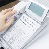
As IP telephony progresses, the demand for telephone switchboards (PBX) that use internet connections is expanding. Use high quality PWBs to achieve clear, reliable communications.
Servers
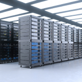
Lincstech’s PWBs make communications speeds faster, further improving server data processing speeds. The major companies supporting the high speed communications industry use these PWBs. Lincstech’s unique technology is at work here, too.
Industrial equipment
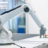
Lincstech PWBs providing both high density wiring and high reliability are an excellent match for industrial machines that propel automation and productivity improvements. Lincstech has a long history of supporting makers across the spectrum in their development work.
