- TOP
- Lincstech’s Strengths
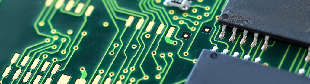
- Surface mount-capable substrate for smaller smartphones and more circuit design margin
Surface mount-capable substrate
for smaller smartphones and
more circuit design margin
The introduction of substrate has
- Increased margin in product design.
- Reduced product size.
- Improved electrical connection reliability of the product.
- Contributed to technological advancement of the industry by adoption in smartphones.
Background of development
The drive to develop double-side mounted modules that leverage high connection reliability and high density mounting

In recent years, increased functionality of components used in smartphones and module miniaturization are advancing at a rapid pace. The technological hurdle for these modules is how much the footprint of the electronic components can be reduced, and developers are seeking technological breakthroughs in this field. To achieve this target, development of PWBs that permit components to be mounted on the surface drew significant attention.
“Can we develop double-side mounted modules that leverage high connection reliability and high density?” “If we do that, we can make modules smaller than ever and give customers more margin.” “This will open new possibilities for circuit design.” This is the kind of conversation that motivated product development.
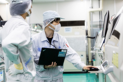
Problems and solutions
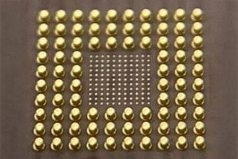
The first challenge was high density bump pitch
The technology that had made conventional double-side mounted modules possible was System in Package. But that used solder to connect external terminals. Limitations on solder ball diameter and soldering pad diameter made further reduction in the pitch of the external terminals difficult.
This caused engineers to turn their attention to developing substrates with copper bumps for double-sided mounting.
Bump pitch alone is not the answer
The next hurdle was improving the bump formation process
In the samples produced in the initial stage of development, the excellent bond strength between the copper bump and pad electrodes was improved, but there was a large variation in bump height.
Without addressing this, realization of high density double-side mounted modules excellent in all aspects would be difficult. It would be necessary to reconfigure one of the fundamental technologies: the plating process.
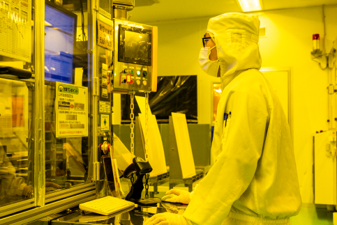
The key to the solution is the integration of all of our knowhow for many substrate types.
In the course of module board development, Lincstech developed high aspect ratio plating and filled plating for layer to layer connections that could be used to form external terminals.
Engineers wondered if they could improve and implement these technologies developed by Lincstech to realize higher density double-side mounted substrates, and proceeded with development. Based on the above elemental technologies, an optimal copper bump formation process was developed, and double-side mounted modules were created that allowed the customer more margin in the circuit design.
Other development stories


Products
We have a broad variety of high-feature substrate and printed wiring boards.
Let us produce substrates for you that match your desired material, application and design.
