- TOP
- Lincstech’s Strengths
- Challenging development of substrates with cavities
Challenging development
of substrates with cavities
The introduction of substrate has
- Achieved smaller and denser substrates with cavities.
- Expanded mounting options by improving design margin.
Background of development
Cavity substrate for even higher processing precision and design margin
Cavities in substrates are created by carving a stepped area around a hole. There have been many cases of forming cavities in strong and easy-to-process ceramic substrates, but this was generally not applied to thinner substrates.
But in the modern society where electronics devices need more functionality in a smaller size, the required board complexity continues to increase. In order to give our customers more design margin in their product development, we set out to develop a cavity process for substrates.
Problems and solutions
The precision needed to make complex cavities was a hurdle

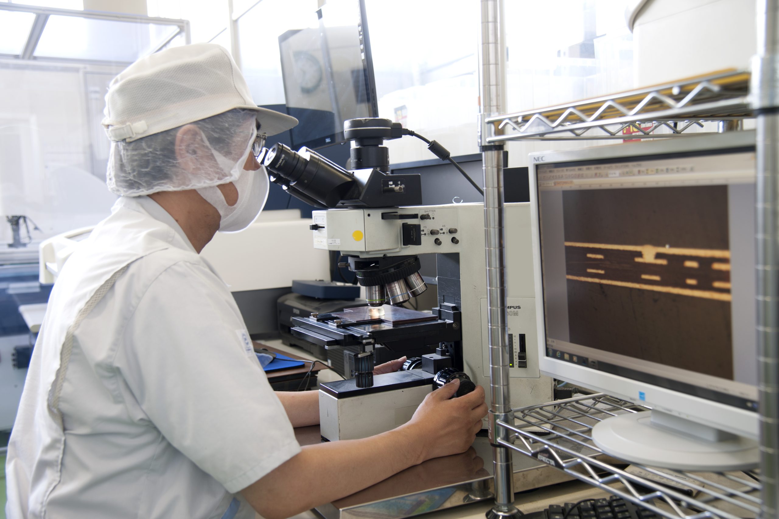
The issue was the difficulty of forming a cavity structure in a substrate. Because substrates are usually made by stacking extremely thin internal circuit layers, even the slightest lack of precision makes it impossible to make cavities. In order to make cavities, it was necessary to completely revise the design rules and production process.
The unprecedented level of required precision in dimensions and process made development extremely difficult.
Employing our specialized technology to clear the hurdles and achieve compactness and multi functionality
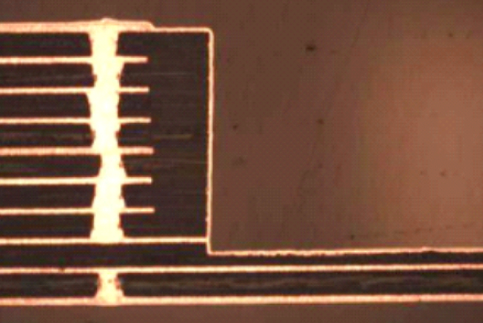
Substrates with cavities were realized by a fusion of a variety of substrate processing and materials technologies. Cavities that appear smooth even under a microscope are the product of a combination of specialty elemental technologies and processes developed over many years of close cooperation with our customers.
Substrates make 3D structures possible
Helping customers make their products more compact

Cavities have improved design margin, which in turn has allowed for further module miniaturization and increased functionality. This is the development story of the substrates that have answered the customers’ demands for “smaller” and “high precision” in their modules, sensors, LEDs and other products.
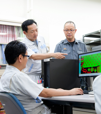
Other development stories


Products
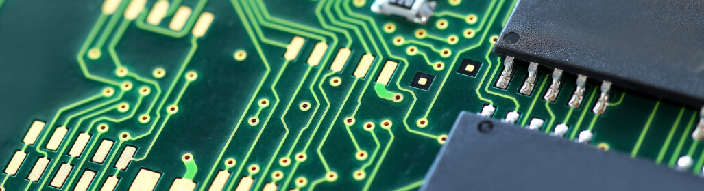
We have a broad variety of high-feature substrate and printed wiring boards.
Let us produce substrates for you that match your desired material, application and design.
