- TOP
- Lincstech’s Strengths
- MWB (Multi wiring board): Astonishingly high density made possible by master level skill
MWB (Multi wiring board):
Astonishingly high density
made possible by master level skill
The introduction of PWB has
- Signal line electrical resistance reduced up to 70% compared with conventional signal lines.
- Astonishing degree of integration possible - 2 ~ 3 times the density of typical multi layer wiring boards.
- Electrical characteristics measured values agree well with the theoretical values, making it easy to achieve the desired characteristics.
- Total development time, including design time, can be shortened.
Background of development
Used for PWB that demand high reliability
"Premium" PWBs
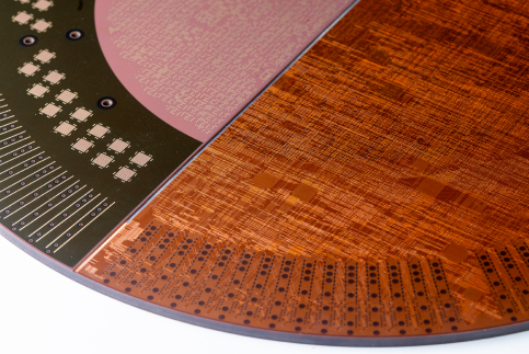
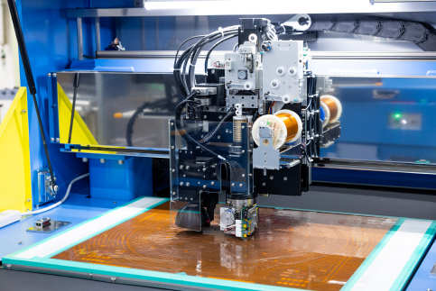
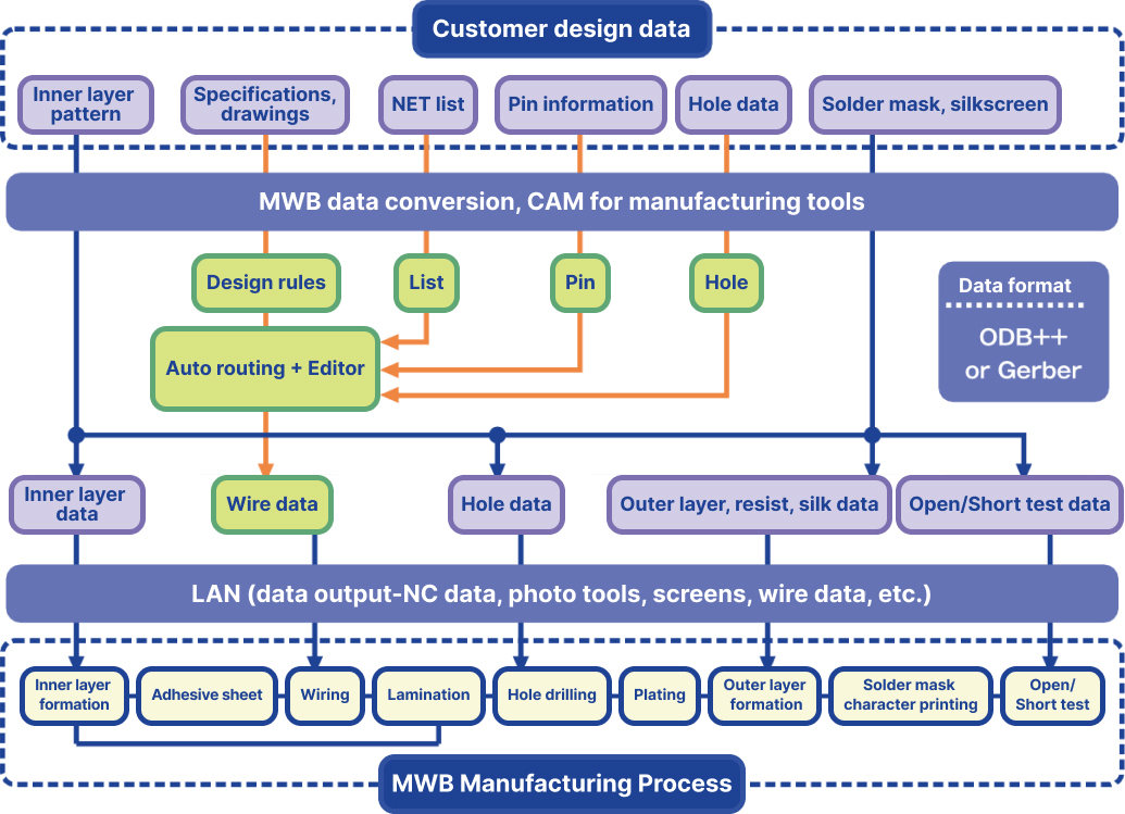
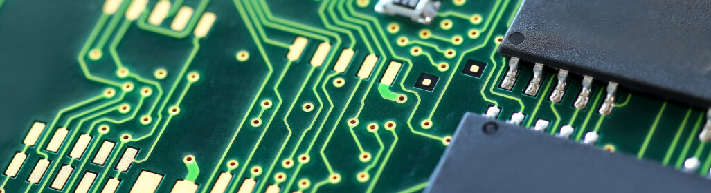
Multi wiring boards (MWB) are unique PWBs that use copper wires for the signal lines. Unlike typical PWBs made by etching, the circuit is formed by using a computer-controlled wiring machine to embed polyimide-coated insulated copper wires into insulation layers.
In MWB, wires with cores of only 0.050~0.10mm in diameter are wired one by one, resulting in signal line resistance per 254mm up to 70% less than that of conventional PWBs, while allowing more complex wiring layouts. We might call MWB “premium” PWBs.
MWB are used in semiconductor inspection equipment, probe cards, switchboards, high-end computers and other applications needing high reliability wiring boards. We continue to push the boundaries of this technology.
Problems and solutions
2~3 times the wiring density of typical multilayer boards
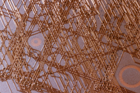
MWB’s strength is that it allows 2~3 times** the wiring per layer when compared to typical multilayer boards. Insulated copper wires allow for wires to cross, resulting in high density wiring, which in turn allows the number of layers to be reduced.
High density wiring in limited wiring space allows higher precision in wiring length and reduction in number of layers of wiring. Hybrids with multi layer boards are also possible.
** Compared with our other products or based on our measurements; Not a guarantee.
Easy matching of electrical characteristics theoretical and actual values
Stable characteristic impedance
Because MWB uses uniform copper wire (±3μm tolerance) in the signal lines, it is easy to match electrical characteristic theoretical and actual values (Standard Zo ±3Ω). The ease of realizing the desired characteristics during development is a strength. In particular, the lot-to-lot variability of Zo is small, allowing for stable electrical characteristics.
High ease of design shortens development time
With MWB, wiring design that takes advantage of its electrical characteristics is easy, allowing total development time, including design time, to be shortened. In addition, the high degree of design margin and ease with which changes to the wiring can be made allows the design process to be made even shorter.
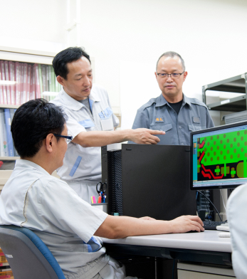
Total design and technical support
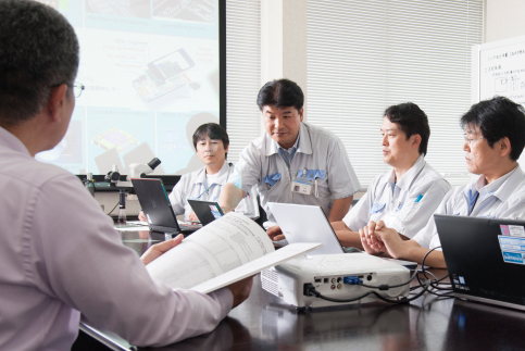
Lincstech’s unique team structure has our technical support staff working together with our sales staff from the very beginning of the development process, allowing us to offer a solution that makes the most of the MWB technology.
Our highly experienced engineers and designers, with their rich experience in development support, are another of our strengths. They can help resolve difficult issues and give guidance on how to make a product a reality.
Development support with a compatible design interface
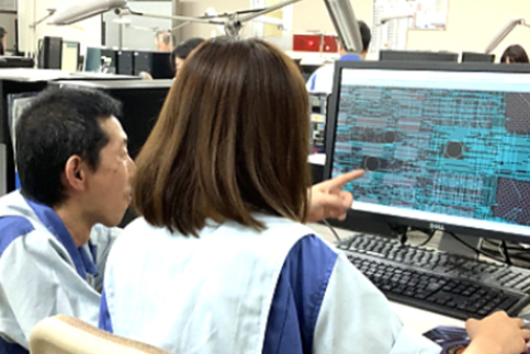
Lincstech’s design interface, which allows existing multi layer wiring designs to be easily converted to MWB, is yet another strength.
Design validation is easy because we use specialized design software that allows wiring design data ODB++ and Gerber files to be read into the customer’s CAD. Multi layer wiring board signal wiring patterns can also be converted easily to MWB wiring patterns**.
** In addition to the usual multi layer wiring board data, please provide part layout and netlist, CAD and other data.
MWB design example
(CAD interface)
MWB specification example MWB uses uniform 65μm wires to achieve ultra-high layer count and high wiring density.
MWB uses uniform 65μm wires to achieve ultra-high layer count and high wiring density.
※The table can be viewed by scrolling left and right.
| Item | Units | Specification | |
|---|---|---|---|
| Wiring density | – | Max.1wire/0.65mm Max.2wires/0.8mm Max.3wires/1.00mm |
|
| Wire diameter | μm | φ100,φ80(tolerance±3μm) φ65(tolerance±2μm) |
|
| Wiring layer count | Layers | 2 ~ 20 layers (MLB 6 ~ 50 layers) | |
| Power, ground layer count | Layers | 2 ~ 42 (for a 7.4mm board) | |
| Maximum product size | mmxmm | 600×550 | |
| Maximum board thickness | mm | 6.3 | 7.4 |
| Minimum drill diameter | mm | φ0.25 | |
| Characteristic impedance | – | ±5~10% | |
| Isometric length wiring | – | Tolerance±1.27mm | |
| Crosstalk | – | <2 %(Tr=1ns) | |
Other development stories


Products
We have a broad variety of high-feature substrate and printed wiring boards.
Let us produce substrates for you that match your desired material, application and design.
