- TOP
- Lincstech’s Strengths
- No restrictions on the form of the customer’s development A new board-to-board connected PWB
No restrictions on the form
of the customer’s development
A new board-to-board connected PWB
The introduction of PWB has
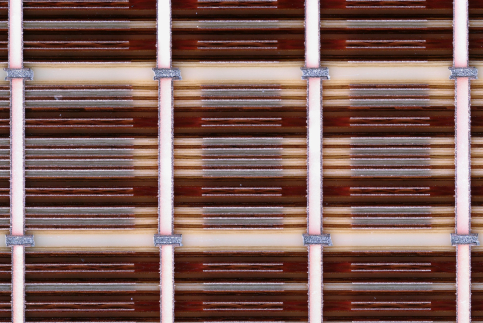
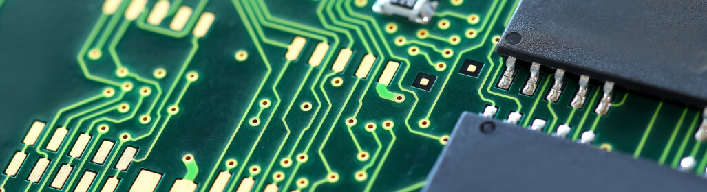
- Holes typically connected by through holes can be split up and unnecessary holes removed.
- Divided boards can be made thinner, and holes even smaller.
- The region where wires can pass is expanded, increasing the amount of wiring in a given space.
- Current no longer flows through unnecessary holes, increasing signal speed.
Background of development
Highly integrated multilayer boards that exceed conventional multi wiring boards (MWB) have become a necessity
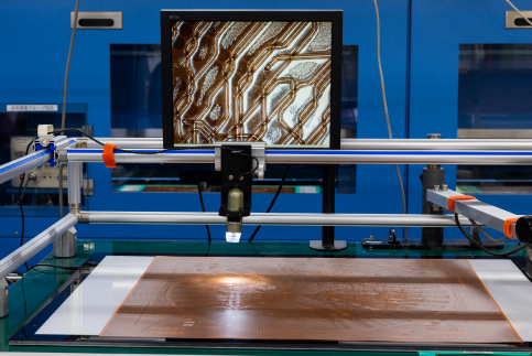
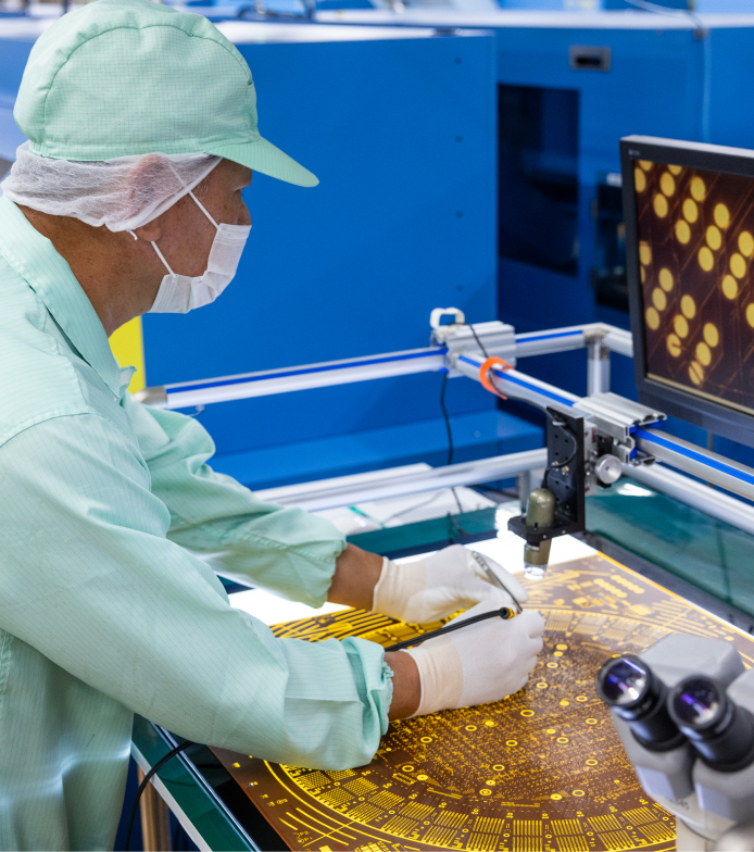
Lincstech manufactures both typical multilayer boards (MLB) and multi wiring boards. Unlike MLB, where circuits are formed by etching copper, MWB uses our original technology copper wires to form the circuits.
Because MWB uses insulated wires, crossing wires in the same plane is possible, allowing more wires to be fit in a given volume. The result is a level of high density that is difficult with MLB. But with advances in PWB manufacturing technology, ultra high layer counts, and smaller hole pitch, MLB density is now encroaching on areas possible only with MWB. On the other hand, higher layer counts with MWB were difficult, placing a limit on how much wiring could be packed into the board.
With this background, customers using Lincstech’s MWB asked us if we couldn’t increase wiring density even further. So we set to work developing a new technology to meet these demands.
Problems and solutions
Breaking away from conventional construction to achieve even higher density
In conventional multilayer boards, holes are formed where electrical connections are needed and the inner walls plated with copper. But what Lincstech and our customers wanted was multi wiring boards with higher density. We would have to break away from conventional construction.
To achieve this, Lincstech proposed splitting the board into 2 or 3 parts in the thickness direction and applying conductive materials as needed with an “inter board joint structure” to electrically connect the upper and lower boards. We set to work on development.
Starting in unfamiliar waters, a process of trial and error to answer customer needs
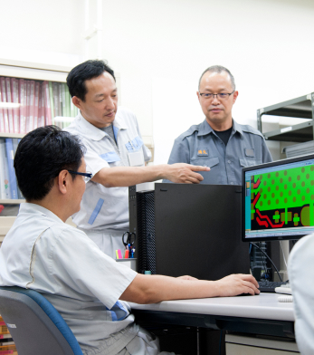
No one at Lincstech had ever considered an inter layer joint structure, and we had to start with selecting the connection materials and inter layer insulation material. For that reason, when we started development, we didn’t limit ourselves to the knowledge we had in house; we supplemented our in-house expertise with expertise borrowed from other companies.
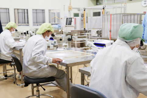
Each material has various requirements on its characteristics. So, in considering the materials, we conducted many material properties evaluations, made many prototypes, and held many meetings inside and outside the company.
Depending on design parameters like thickness of the connection face and size of the connecting materials, we had many issues like poor connections (opens), unwanted contact between adjacent connecting materials (shorts), and so on. It took much discussion among Lincstech engineers over the connecting face design specifications to resolve the issues and finally make a finished board. But, while Lincstech has the capability to evaluate basic electrical characteristics in house, we are unable to evaluate them under the real-world conditions seen by the customers. Our customers helped us to evaluate the boards, and thus PWBs using a new inter layer joint structure were born.
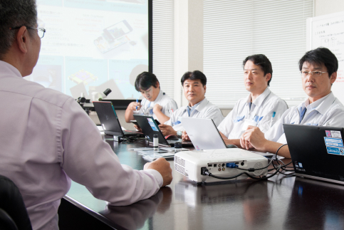
Board to board connected PWBs were made possible by close cooperation with our customers. The development went smoothly because our development people accompanied our sales people to customer meetings, allowing us to have detailed technical discussions from the outset.
We don't put restrictions on the form of the customer's development
The PWBs are completed
Lincstech’s original multi wiring board (MWB) technology is exclusive to us, and some of the materials used have no general applicability. Diverse knowledge and technology was necessary in the materials, design and manufacture. Our experience in developing MWB with our commitment to “create new PWBs that would place no restrictions on the form of the customer’s development” was instrumental in developing the board to board connected PWBs.
With the practical use of the inter layer joint structure, the amount of wiring that can be packed into MWB increased dramatically, once again allowing a level of high density wiring that MLB can’t match. Even in semiconductor inspection equipment, where MWB is most often used, the number of inspections that can be done simultaneously has increased and the inspection lead time shortened. The customers’ margin in design has also improved dramatically, so you might call this the birth of a PWB that contributes to improvement of PWB characteristics more broadly.
Other development stories

Products
We have a broad variety of high-feature substrate and printed wiring boards.
Let us produce substrates for you that match your desired material, application and design.
