- TOP
- Lincstech’s Strengths
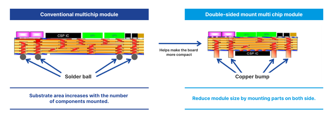
- Substrates with copper bumps reduced module size
Substrates with copper bumps
reduced module size
The introduction of substrate has
- Improved circuit design margin by mounting semiconductor chip on substrate to and bottom surfaces.
- Allowed modules to be more compact with higher functionality.
- Improved connection reliability and heat dissipation for better semiconductor chip cooling.
Background of development
Richly-featured smartphones demand compact, multi-functional modules

As smartphones become more feature-rich, the modules inside them must incorporate more functions. At the same time, increasing battery capacity and size reduce the space available for the modules. One way to solve the problems associated with increasing module functionality while decreasing their size is to make use of substrates that make multi chip modularization possible.
Multi chip modularization was made possible by copper bump substrates developed by Lincstech.
Problems and solutions
Copper bump substrates reduce module substrate size
By using copper bumps as the external terminals, copper bump printed wiring boards allow the external terminations and chips to be mounted in the same surface. Mounting semiconductor chips on the substrate top and bottom surfaces allows modules to be more compact with increased functionality.
Conventional modules used solder balls as the external terminals that connect the module to the board. The difficulty in controlling the shape of the solder balls restricted the gap height between module and main board and external terminal pitch.
For copper bump substrates, the use of pattern copper plating technology allows the shape to be controlled in 0.01mm increments. As a result, improvements in circuit design margin, such as putting chips in the same plane as the external terminals and reducing bump pitch to as little as 0.31mm, are possible.
Size reduction of multi chip module substrate
Creation of a multi chip module with high connection reliability and heat dissipation characteristics
Comparison of solder and copper heat dissipation(reference range)
※The table can be viewed by scrolling left and right.
| Material | Measurement temperature[K] | Specific heat capacity [J/(kg・K)] |
Thermal conductivity [W/m・K] |
CTE[10-6/K] | Bump strength [g/φ0.22mm] |
|---|---|---|---|---|---|
| Copper | 293 | 419 | 372 | 17.7 | 430 |
| Solder (50Sn) |
293 | 176 | 49 | ー | ー |
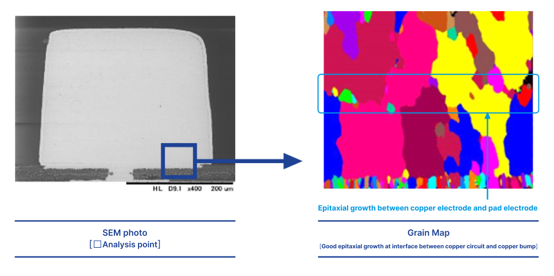
Joint between the copper bump and copper circuit
Other development stories


Products
We have a broad variety of high-feature substrate and printed wiring boards.
Let us produce substrates for you that match your desired material, application and design.
