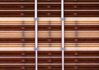
Board to board connected PWB
Unnecessary through holes are replaced by IVH, allowing wiring in areas that were restricted in conventional boards
for improved design freedom and ability to fit more wires into the space. Ultra-high layer counts and
board thicknesses of 10mm and more are also possible.
Product Outline
- Small hole diameter allows more space for wiring between holes.
- More space for wires means a large improvement in wiring design freedom.
- Thicker boards can be achieved easily.
- Signal wiring densities not possible with MWB (multi wiring boards) achieved.
- IVH stubs are minimized for to allow higher speeds.
Even higher speeds are possible when combined with inner back drilling.
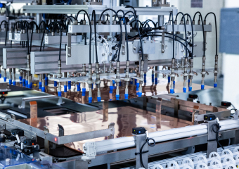
Manufacturing locations:Shimodate Plant
Features
01 Improved wiring design margin and dramatically increased number of wires in a given area
By replacing through holes with IVH, hole diameter can be reduced, allowing more wires to be placed between holes. And unnecessary through holes are removed (only necessary vias are replaced with IVH), increasing the space for wiring and greatly improving wiring design margin.
02Higher speed
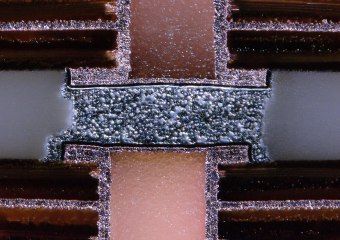
Combination of IVH stacked structure and inner back drilling
By placing IVH in a stacked structure, the stubs produced by conventional vias are minimized, allowing for high speed operation. Even higher speeds are possible if combined with inner back drilling.
03Ultra-high layer counts and high board thickness not possible with conventional manufacturing processes
Limitations on manufacturing equipment and product specifications (hole diameter, copper plating, etc.) restricted maximum thickness to 7.7mm. With this technology, thickness in excess of 7.7mm is made possible by first making sub boards, and then stacking them with conductive paste between the boards to connect them. At the same time, ultra-high layer counts of over 100 layers are made possible.
04An environmentally-friendly process
Compared to conventional PWBs with mixed through holes and IVH, board to board connected PWBs made with IVH need fewer copper plating steps. And by performing electrical inspection of the sub boards at the time they are finished, problems can be detected at an early stage and defective PWBs discarded, reducing the overall waste, resulting in an environmentally-friendly process.
Technology roadmap
【Multi Wiring Board】
*The table can be viewed by scrolling left and right.
| Item | 2024 | 2025 | 2026 | |
|---|---|---|---|---|
| Book Count | 2 Books |
≦ t7.4mm |
||
| 3 Books |
≦ t7.4mm |
≦ t12.0mm |
||
| Connection min. Pitch |
0.80mm |
0.65mm |
||
| Routing density |
2 wires / 0.8mm , 1 wire / 0.65mm (Φ0.065 wire) |
|||
|
2wires/0.7mm (Φ0.050 wire) |
||||
| Min. Drill dia. |
Φ0.25 (Φ0.065 wire) |
|||
|
Φ0.20 (Φ0.050 wire) |
||||
【Multi Layer Board】
*The table can be viewed by scrolling left and right.
| Item | 2024 | 2025 | 2026 | |
|---|---|---|---|---|
| Book Count | 2 Books |
≦ t7.4mm |
||
| 3 Books |
≦ t7.4mm |
≦ t12.0mm |
||
| Connection min. Pitch |
0.80mm |
0.65mm |
||
| Min. Drill dia. |
Φ0.20 |
Φ0.15 |
||
Typical applications
Probe cards
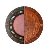
Probe cards are fixtures used to check the quality of wafers used in the semiconductor manufacturing process. The importance of inspection precision is increasing along with semiconductor demand. Lincstech’s printed wiring boards have the top share in semiconductor inspection processes.
