- TOP
- Topics
Topics
What are printed
wiring boards?
We explain what printed PWBs are,
their role, and what products they are used in.
-
2025.01.09 Basic Knowledge of PWBs
What is a PWB? Differences from the printed circuit board (PCB), types, and manufacturing processes
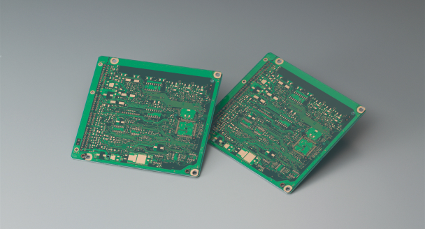
PWBs are used in almost all products that run on electricity like cars, home appliances, computers, industrial devices and have made a large contribution to the compactness and high functionality of electronics products. On this page, to establish a basic level of PWB knowledge, we explain the difference between PWBs and printed circuit boards (PCBs), materials, number of circuit layers, types by structure, and manufacturing processes. There is large variation across the industry in the explanation of PWBs, but we adhere to JIS (Japanese Industrial Standards) and other public standards as much as possible. Please use this as a reference when considering PWBs for your products. Contents 01What is a PWB? The difference between PWBs and printed circuit boards The difference between PWBs and semiconductors 02PWB's role 03PWB types Classification by material Classification by circuit layer count 04PWB applications 05PWB manufacturing process 06Summary 01What is a PWB? PWB is an insulating substrate with circuits formed of copper foil or other conductive materials on the outer surface and inside. In order to differentiate from a board after parts are mounted on it, the pre-mounted state is often referred to as a "bare board". It's most easily explained as the green board in electronics products with a lot of electronic parts attached to it. The board without the parts is the PWB.The PWB supplies electricity to the resistors, capacitors, IC packages and other parts mounted to it, as well as transferring electronic signals, and is an essential component in electronics products. PWBs are used in cars, home appliances, computers, robots - almost all products that run on electricity. The difference between PWBs and printed circuit boards Terms similar to PWB include printed circuit board (PCB) and printed substrate, but each has a different definition, so it’s important to be aware of these differences. Printed circuit board is a general term for both PWBs that have electronic components mounted on them and are operational as electronic circuits, and PWBs without those components. Printed circuit boards play a critical role in electronic devices, transmitting power and signals and enabling the mounted electronic components to function. Additionally, the names of the typical component parts of PWBs are as follows: Pattern The shape formed on the PWB. Both conductive and non-conductive areas are referred to as patterns. For example, the conductor (usually copper) wiring (circuit) area formed surface or inside the board are patterns. Lead (Pin) The leg part of a component mounted on the PWB. Electricity or electric signal is supplied to electronic components through these legs. Plated Through-Hole (PTH) A hole with metal deposited on the walls used to electrically connect the front and back sides of the PWB. PTH is sometimes used as an abbreviation. It is also used as a hole for inserting leads (pins) and attaching components for electrical conduction. Land A conductive pattern used for mounting and connecting components. It serves as a contact point to reinforce through-holes, connect through-holes to patterns, or electrically connect the terminals of electronic components. Pad A land for surface-mounted components. It serves as a contact point to electrically connect the terminals of electronic components with the circuit pattern on the PWB. By connecting electronic components to the plated through-holes and pads, a printed circuit board is formed.If you think of a PWB as the general term for boards that are operational as electronic circuits and "printed substrate" as an unofficial term, it becomes easier to understand the differences between them. The difference between PWBs and semiconductors A component closely related to PWBs is the semiconductor. A semiconductor is a material like silicon that is between the “conductor” and “insulator” in ability to conduct electrical current. It also refers to electronic components made from these materials, such as transistors, diodes, and integrated circuits (ICs).An integrated circuit (IC) is a circuit that integrates the functions of electronic components like transistors, resistors, capacitors, and diodes onto a small chip made of semiconductor materials like silicon. It is characterized by its ability to perform tasks such as calculation, storage, and sensing on a single chip.Like PWBs, ICs form electronic circuits, but they differ significantly in materials, size, and functionality. Integrated circuits (ICs) are essential for precision electronic devices like computers and are commonly seen attached to PWBs as black components (packages) equipped with numerous metal terminals (leads or electrode pads).PWBs are crucial components that supply power and transmit electrical signals to electronic components made of semiconductors, enabling the operation of electronic circuits. 02PWB's role PWBs serve to electrically interconnect electronic components and supply power while also securing each component in place.Before the invention of PWBs in 1943, the process of creating electronic devices involved manually wiring components together and soldering them to terminal lugs mounted on a chassis. This process of soldering each component one by one required a lot of time and effort, leading to wiring mistakes. Additionally, if the soldering was not done properly, the connections would be unstable, resulting in malfunctions.The invention of PWBs made it possible to easily connect and arrange electronic components, allowing for the mass production of products with stable quality in less time and with less effort. Moreover, the ability to efficiently organize electronic components in a compact space, combined with the miniaturization and enhanced performance of electronic parts, greatly accelerated the development of electronic devices, bringing significant benefits to society.Today, PWBs are indispensable to modern electronic devices. 03PWB types PWBs are classified by materials used, circuit layer count, and structure. Below, we explain the PWB types by category. Classification by material When classifying PWBs by material, the following are the four main types: Rigid PWB (Rigid PCB) A PWB formed by creating a conductor pattern on a rigid insulating substrate using copper-clad laminates. Copper-clad laminate refers to a board in which a sheet, made by impregnating a base material such as paper or glass cloth with resin, is laminated and subjected to pressure and heat treatment, with copper foil applied to both sides. Many PWBs fixed in electronics device cases are rigid PWBs. Their advantages include sturdiness, high durability, and ease of component mounting. They are widely used in various electronic products. Flexible PWB(Flexible PCB, Flex PCB) A PWB where a conductor pattern is formed on a flexible, insulating film made of materials like polyester or polyimide. These are used in devices that require assembly into complex shapes or in the moving parts of machines. They are also used in the bending sections of laptops and mobile phones. Flex-Rigid PWB(Rigid-Flex PCB) A PWB that combines rigid PCBs with flexible PCBs, offering both the rigidity of a rigid board and the flexibility of a flexible board. It consists of a rigid part for mounting components and a flexible part that can be bent or stretched. These are commonly used in electronics that require durability against vibration or shock, such as industrial cameras or printers, and in devices with moving parts. Metal Core PWB(Metal-Based PCB, Metal-Core PCB) A PWB that uses a metal plate as the supporting structure for its components. These boards have a structure where a rigid PCB is mounted on a metal plate, typically aluminum or copper, which has high heat dissipation properties. There are various types depending on the material used, such as aluminum-based or copper-based PCBs. They are used for heat sinks or as the power layer in devices. Classification by circuit layer count The amount of wiring that can be placed on a single PWB is limited. However, as electronic devices continue to evolve, the number of required circuits has increased. To address this, multilayer PWBs were developed, allowing multiple layers of circuits to be created within a single board, increasing wiring density. The classification of PWBs by the number of circuit layers is as follows: Single-Sided PWB(Single-Sided PCB) A PWB with the conductor pattern printed on only one side. Since there is wiring on only one side, complex wiring patterns cannot be created, limiting the number of components that can be mounted. However, it offers the advantage of lower manufacturing costs. Double-Sided PWB(Double-Sided PCB) A PWB with conductor patterns printed on both sides. Holes are drilled into the board, and copper plating connects the top and bottom layers, allowing for three-dimensional wiring patterns. This allows for more components to be mounted compared to single-sided boards, enabling further miniaturization and improved performance. Multilayer PWB(Multilayer PCB) A PWB with three or more conductor layers. Holes are drilled and copper plating is used to electrically connect the surface and inner layers. The ability to arrange the wiring in complex, three-dimensional patterns increases wiring density, allowing more components to be integrated mounted onto a single board compared to double-sided PWBs. Multilayer PWBs can be further classified into several types, including the following: General Multilayer PCB (Medium to Low Layers)A common type of multilayer PWB made by stacking insulation and conductor layers. Through holes are drilled, and copper plating connects the layers. High-Layer, High-Density Multilayer PCBAt Lincstech, multilayer PWBs with 20 or more layers are called "high-layer, high-density PWBs." These highly dense, high-functionality boards can accommodate numerous circuits and are mainly used in complex electronic devices like servers, network equipment, and semiconductor testing devices. Build-Up Multilayer PWB (Build-Up PCB)A multilayer PWB where insulation and conductor layers are stacked and connected layer by layer. Since laser-drilled holes can be made smaller than standard through-holes, higher wiring density can be achieved, reducing the overall board size. These are often used in compact and multifunctional electronic devices Multi-Wiring Board(MWB)A product that uses Lincstech's proprietary technology, this multilayer PWB forms circuits using copper wires with insulating coatings. Multiple wires can overpass within the same layer, allowing for increased wiring density in each layer. As a result, it can accommodate far more wiring than standard multilayer PWBs with the same thickness and number of layers. Additionally, the use of copper wires with a uniform diameter ensures more stable performance with less variation compared to conventional multilayer PWBs. High-Layer, High-Density Multilayer PCB Build-Up Multilayer PWB (Build-Up PCB) Multi-Wiring Board(MWB) 04PWB applications PWBs (PCBs) are used in nearly all electrical devices. Below are some common examples: Measurement devices Satellites Medical devices Robots Game machines Computers IT devices Semiconductors LED Automotive Smartphones Industrial robots etc High-density, high-performance PWBs are essential for next-generation devices, such as 5G/6G communication equipment, self-driving vehicles, and industrial machines equipped with AI for automation. In addition, products like lighting devices and automobiles are becoming increasingly electric, leading to the use of PWBs in areas where they were previously unnecessary.There is also a growing demand for PWBs in new fields, such as service robots (e.g., delivery robots), care devices, and wearable technology. As future generations of electronics demand more complex functions, the need for higher density and more advanced PWBs will continue to rise. 05PWB manufacturing process PWBs (PCBs) are precision components that require specialized manufacturing techniques. Below is an explanation of the typical process for manufacturing multilayer boards using the subtractive method. 【1】A substrate made of copper foil and an insulating layer (resin) called a copper-clad laminate is laminated with a photosensitive film (dry film). A negative film of the wiring diagram is overlaid, and the board is exposed to light. Only the parts of the film exposed to light harden. 【2】After developing, where unexposed parts of the dry film are removed with a weak alkaline solution, an acidic solution is used to dissolve the exposed copper (etching). The remaining copper forms the circuit. The hardened dry film on the copper circuit is then removed with a strong alkaline solution, forming the inner layer. 【3】An automated optical inspection machine scans the inner layer circuit and compares it to the design data to check for defects. 【4】The inner layer is stacked with insulation layers (adhesive layers) and copper foil. The multilayer board is laminated by press, then drilled. Copper plating forms plated through-holes that electrically connect the layers. 【5】The board is laminated with dry film again to create the outer layers, similar to the inner layers. An automated optical inspection machine compares the circuits to the design data to ensure there are no defects. 【6】A solder mask ink is applied to protect the circuits from solder when mounting components. After exposure and alkaline development, areas like pads and through-holes are left exposed, and the solder mask is cured by heat. 【7】The board is shaped by outer routing or press machining into the final form required by the customer. After electrical inspection, surface treatment (such as solder coating or pre-fluxing) is applied to prevent corrosion. 【8】The final board undergoes automated visual inspection, open/short test, and manual visual inspections. Once the quality is confirmed, it is packed and shipped. 06Summary PWBs are indispensable components in electronic products which provide a mounting surface for electronic components and connect the components electrically. In addition to being classified according to material and structure as rigid, flexible and flex-rigid, they can also be classified by circuit layer count as single-sided, double-sided, and multilayer. High-density and high-performance PWBs are essential components for 5G/6G communication devices, self-driving vehicles, and AI-driven industrial equipment. Going forward, PWBs will continue to be important components in supporting the next generation of technology.
